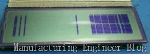
Recently we found many missed segment defect for the HSC (Heat Seal Connector) solution LCM. As experience tell me the reliability of HSC bonding process is not good for the industrial product. It is easily to miss-contact between the PCB and HSC after a period of use.
I only know the result but I didn’t know why in the past. In order to understand why the HSC bonding force is not good and trial to fix this kind of defect, I collect some information from expert and supplier and study the root cause.
Below is the notice items I get from HSC supplier and expert:
- The HSC is temperature and humidity sensitive component. If store the HSC under high temperature or high humidity environmental then the adhesive propriety will be degraded.
- HSC supplier asks the bonding width shall have 3.0mm to guarantee its bonding force meet requirement. Unfortunately, many new product design only keep the 1.5~2.0mm bonding width and this may bring lower bonding force and weak the reliability.
- Why always found the HSC be peeled off on the PCB side and not the glass side?
- The potential reason is the PCB gold finger may not smoothly enough and HSC can’t be bonded on the PCB well. Or may be the gold finger pad higher than the space between gold finger pads. This is probably what causes the rippling effect we’ve noted. There is potential that the hot melt resin does not flow into the crevices or if it flows too much it would leave some thinner layers of adhesive in some areas (especially the peaks, that is, the finger pads).
- Adding solder mask between the gold finger pads to improve the flatness of PCB golder finger. - HSC supplier won’t recommend applying a continuously stress or bending force to the bonding area. This will make the bonding damage after period use.
- Sometimes we will find there is misalignment issue between the HSC and substrate since almost the HSC is bonded by semi-auto machine and alignment by CCD by manual. The misalignment will not affect to the bonding force. The only affect is the conductive resistance only. As HSC supplier claimed that keep 20~30 pcs of graphite pixels per trace on the bonding trace will be OK.
- The adhesive of HSC shall be transferred to the substrate once it is peeled off by force for the good bonding on HSC. So we can check the yellow adhesive is transferred to substrate or not while inspect the defect sample or test the peeling off for adhesive strength
By the way, most of the critical parameter shall be controlled during manufacturing.
- Measuring the temperature profile by real-time thermal couple on the substrate.
- Using pressure meter to check the bonding pressure force and not only checking the air cylinder.
- Making sure the thermal wedge is evenly and well press on the substrate before bonding process.
- 1st bonding sample must be implemented the HSC peel off adhesive strength test and pass specification. Also check the adhesive must keep on the substrate while peel off the HSC.
Related article:
PTF(Polymer Tick Film) process introduction
Hot-Bar Flex cable Design Notices
Flex cable(FPC) Trace Pattern Layout Design Notices


This is great information. I learned a lot here.
ReplyDeleteInjection Molding Service